MycelioTronics: Biodegradable Electronics Substrates from Fungi
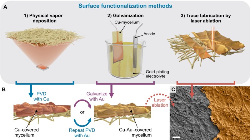
A notated illustration showing how a mycelial network may be functionalized as a PCB substrate. The process starts with Cu vapor deposition onto the network followed by Au either by more vapor deposition or electrodeposition. Traces are then cut via laser ablation.

E-waste is one of the main unfortunate consequences of the widespread adoption of electronic devices, and there are various efforts to stem the flow of this pernicious trash. One new …read more Continue reading MycelioTronics: Biodegradable Electronics Substrates from Fungi
Hackaday Links: November 1, 2020

We normally chuckle at high-profile auctions where people compete to pay as much as possible for items they clearly don’t need. It’s easy to laugh when the items on the block are things like paint-spattered canvases, but every once in a while some genuine bit of history that really piques …read more

Continue reading Hackaday Links: November 1, 2020

Component Shelf Life: How To Use All That Old Junk

There are two types of Hackaday readers: those that have a huge stock of parts they’ve collected over the years (in other words, an enormous pile of junk) and those that will have one a couple of decades from now. It’s easy to end up with a lot of stuff, …read more

Continue reading Component Shelf Life: How To Use All That Old Junk

The components are INSIDE the circuit board

Through-hole assembly means bending leads on components and putting the leads through holes in the circuit board, then soldering them in place, and trimming the wires. That took up too much space and assembly time and labor, so the next step was surface mount, in which components are placed on top of the circuit board and then solder paste melts and solders the parts together. This made assembly much faster and cheaper and smaller.

Now we have embedded components, where in order to save even more, the components are embedded inside the circuit board itself. While this is not yet …read more

Continue reading The components are INSIDE the circuit board

How to Take Pictures of PCBs

While we’ve covered light box builds and other DIY photography solutions, general picture-snapping tips and tricks are a bit out of the purview of what we normally write about. Nevertheless, [Alain] just put up a great tutorial for taking pictures of PCBs. This is a great skill to have — no one cares about what you’ve built unless you have a picture of it — and the same techniques can be applied to other small bits and bobs of electronic equipment.

As with all matters of photography, light is important. [Alain] built a DIY light box using two cheap outdoor …read more

Continue reading How to Take Pictures of PCBs

Use All that Extra Space with PCB Panelization

Anyone who’s made a PCB has encountered the conundrum of having to pay for space that you don’t use… for instance, designing a round PCB and seeing the corners go to waste. The solution? Smaller boards added to the blank spots.

One logical stumbling block might be that you simply don’t have a small PCB design ready to go. Latvian hacker [Arsenijs] created a resource of small PCBs that can be dropped into those blank spots, as well as a tutorial on how to combine the gerbers into a single panel.

Great minds think alike, and this guide is following …read more

Continue reading Use All that Extra Space with PCB Panelization