MycelioTronics: Biodegradable Electronics Substrates from Fungi

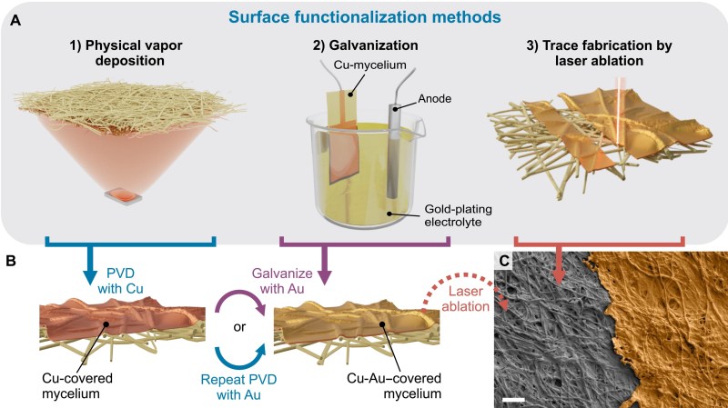
A notated illustration showing how a mycelial network may be functionalized as a PCB substrate. The process starts with Cu vapor deposition onto the network followed by Au either by more vapor deposition or electrodeposition. Traces are then cut via laser ablation.

E-waste is one of the main unfortunate consequences of the widespread adoption of electronic devices, and there are various efforts to stem the flow of this pernicious trash. One new …read more Continue reading MycelioTronics: Biodegradable Electronics Substrates from Fungi

The Woeful World of Worldwide E-Waste

How large is the cache of discarded electronics in your home? They were once expensive and cherished items, but now they’re a question-mark for responsible disposal. I’m going to dig into this problem — which goes far beyond your collection of dead smartphones — as well as the issues of where this stuff ends up versus where it should end up. I’m even going to demystify the WEEE mark (that crossed out trashcan icon you’ve been noticing on your gadgets), talk about how much jumbo jets weigh, and touch on circular economies, in the pursuit of better understanding of the …read more

Continue reading The Woeful World of Worldwide E-Waste