Commodore C64: the Most Popular Home Computer Ever Turns 40

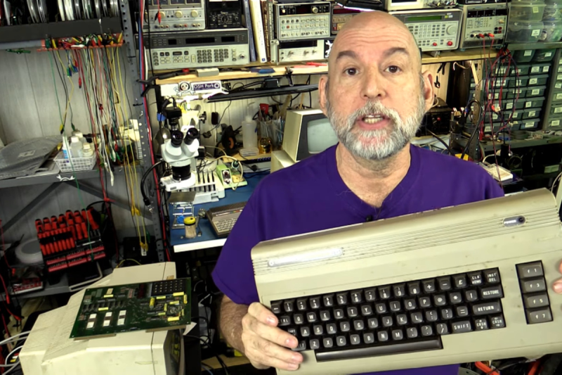
This year marks the anniversary of the most popular selling home computer ever, the Commodore 64, which made its debut in 1982. Note that I am saying “home computer” and …read more Continue reading Commodore C64: the Most Popular Home Computer Ever Turns 40

Saturday: Vintage Computer Festival West

The Vintage Computer Festival West is an annual gathering to celebrate the awesome hardware that ushered in the Information Age. Normally held at the Computer History Museum in Mountain View, California, this year VCF West is happening virtually and it all starts on Saturday!

The lineup of talks looks great, …read more

Continue reading Saturday: Vintage Computer Festival West

Die Photos Reveal Logic from Commodore 128 PLA Chip

The 8721 PLA, or programmable logic array, was one of the chips that had to be invented to make the Commodore 128, the last of the 8-bit computers that formed the leading edge of the early PC revolution, a reality. [Johan Grip] got a hold of one of …read more

Continue reading Die Photos Reveal Logic from Commodore 128 PLA Chip

High-Speed PCB Design Hack Chat with Bil Herd

Join us on Wednesday, September 25 at noon Pacific for the High-Speed PCB Design Hack Chat with Bil Herd!

Printed circuits have become so commoditized that we seldom think much about design details. EDA software makes it easy to forget about the subtleties and nuances that make themselves painfully obvious

…read more

Continue reading High-Speed PCB Design Hack Chat with Bil Herd

Video: Putting High Speed PCB Design to the Test

Designing circuit boards for high speed applications requires special considerations. This you already know, but what exactly do you need to do differently from common board layout? Building on where I left off discussing impedance in 2 layer Printed Circuit Board (PCB) designs, I wanted to start talking about high speed design techniques as they relate to PCBs.  This is the world of multi-layer PCBs and where the impedance of both the Power Delivery Network (PDN) and the integrity of the signals themselves (Signal Integrity or SI) become very important factors.

I put together a few board designs to test …read more

Continue reading Video: Putting High Speed PCB Design to the Test

Inductance in PCB Layout: The Good, the Bad, and the Fugly

When current flows through a conductor it becomes an inductor, when there is an inductor there is an electromagnetic field (EM). This can cause a variety of issues during PCB layout if you don’t plan properly, and sometimes we get burned even when we think we have planned for unwanted inductance and the effects that come with them.

When doing high speed logic we need to be able to deliver sudden changes in current to the devices if we want to have proper switching times and logic levels. Unfortunately inductance is usually not a friend in these circumstances as it …read more

Continue reading Inductance in PCB Layout: The Good, the Bad, and the Fugly