Etching Large Brass Sheets is Harder Than You Think

One of my favorite ways to think of engineering is that a glass is not half empty or half full, only twice as large as it needs to be. As useful as that idea is, it also means that I rarely put any effort into the aesthetics of my projects …read more

Continue reading Etching Large Brass Sheets is Harder Than You Think

Tiny Art Etched into Silicon Wafers with Electron Beam Lithography

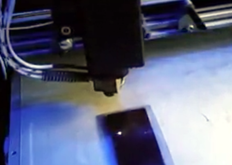
Looks like [Sam Zeloof] got bored on his Thanksgiving break, and things got a little weird in his garage. Of course when your garage contains a scanning electron microscope, the definition of weird can include experimenting with electron-beam lithography, resulting in tiny images etched into silicon.

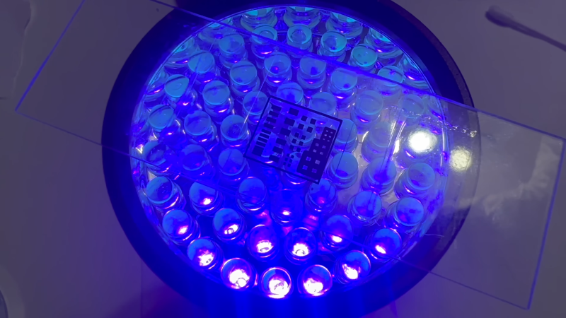
You’ll probably remember [Sam] from his 2018 Hackaday Superconference talk on his DIY semiconductor fab lab, which he used to create a real integrated circuit. That chip, a PMOS dual-channel differential amp, was produced by photolithography using a modified DLP projector. Photolithography imposes limits to how small a feature can be created on silicon, …read more

Continue reading Tiny Art Etched into Silicon Wafers with Electron Beam Lithography

Put that DLP Printer to Use Making PCBs

Now that these DLP printers are cheaper and more widely available, we’re starting to see hackers poking around the edge of the envelope to see what else the machines are capable of. [Electronoobs] recently got his hands on a couple of these printers, and thought he would do some experiments with using them for PCB production.

Rather than extruding molten plastic, these printers use light to cure resin layer-by-layer. In theory if the printer is good enough to cure the light-activated resin for a high resolution print, it should be able to do much the same thing with photosensitive PCBs. …read more

Continue reading Put that DLP Printer to Use Making PCBs

Old Scanner Finds New Life In DIY PCB Fab

Cheap, high-quality PCBs are truly a wonder of our age. That a professionally fabricated board with silkscreen and solder mask can be ordered online and delivered to your door has lowered the bar between a hobbyist project and a polished product. But the wait can be agonizing, and it can throw a wrench into the iterative design process. What to do?

[Andras Kabai] knows the answer to that, and this former flatbed scanner turned into a UV exposer is the centerpiece of his DIY board fab. The old Mustek scanner was a couple of bucks secondhand, and provided not only …read more

Continue reading Old Scanner Finds New Life In DIY PCB Fab

Entry-Level 3D Printer Becomes Budget PCB Machine

A funny thing happened on [Marco Rep]’s way to upgrading his 3D printer. Instead of ending up with a heated bed, his $300 3D printer can now etch 0.2-mm PCB traces. And the results are pretty impressive, all the more so since so little effort and expense were involved.

The printer in question is a Cetus3D, one of the newer generation of affordable machines. The printer has nice linear bearings but not a lot of other amenities, hence [Marco]’s desire to add a heated bed. But hiding beneath the covers was a suspicious transistor wired to a spare connector on …read more

Continue reading Entry-Level 3D Printer Becomes Budget PCB Machine