Inductance in PCB Layout: The Good, the Bad, and the Fugly

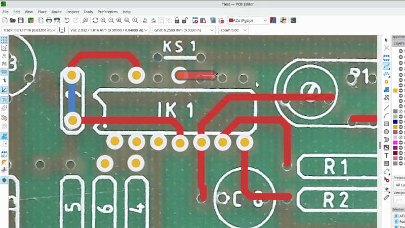
When current flows through a conductor it becomes an inductor, when there is an inductor there is an electromagnetic field (EM). This can cause a variety of issues during PCB layout if you don’t plan properly, and sometimes we get burned even when we think we have planned for unwanted inductance and the effects that come with them.

When doing high speed logic we need to be able to deliver sudden changes in current to the devices if we want to have proper switching times and logic levels. Unfortunately inductance is usually not a friend in these circumstances as it …read more

Continue reading Inductance in PCB Layout: The Good, the Bad, and the Fugly

Learn Advanced PCB Design for $200–Worth It?

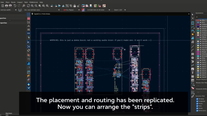
[Helentronica] has been using Altium Designer to lay out PC boards since he was a student. Now as a freelancer, he felt like he didn’t quite know all that he wanted to know. Keep in mind he’d done multilayer boards with BGAs and LVDS routing, so he was no neophyte. He decided to spend about $200 on an advanced course from Fedevel Academy. In this day where everything is free on the Internet, is it worth paying $200 to watch some videos?

[Helentronica] probably weighed the same question. However, he was interested in the course project which is an open-source …read more

Continue reading Learn Advanced PCB Design for $200–Worth It?

PCB Design Guidelines to Minimize RF Transmissions

There are certain design guidelines for PCBs that don’t make a lot of sense, and practices that seem excessive and unnecessary. Often these are motivated by the black magic that is RF transmission. This is either an unfortunate and unintended consequence of electronic circuits, or a magical and useful feature of them, and a lot of design time goes into reducing or removing these effects or tuning them.

You’re wondering how important this is for your projects and whether you should worry about unintentional radiated emissions. On the Baddeley scale of importance:

  • Pffffft – You’re building a one-off project that

…read more

Continue reading PCB Design Guidelines to Minimize RF Transmissions

SKiDL: Script Your Circuits in Python

SKiDL is very, very cool. It’s a bit of Python code that outputs a circuit netlist for KiCAD.

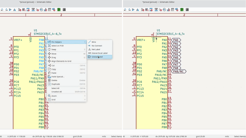
Why is this cool? If you design a PCB in KiCAD, you go through three steps: draw the schematic, assign footprints to the symbolic parts, and then place them. The netlist ties all of these phases together: it’s a list of which parts are connected to which, the output of schematic capture and the input for layout. The ability to generate this programmatically should be useful.

For instance, you could write a filter circuit generator that would take the order, cutoff, and …read more

Continue reading SKiDL: Script Your Circuits in Python

This EAGLE Script Gets Quotes For Your Boards

Weary of manually entering manufacturing parameters into PCBShopper’s web form, [Jeremy Ruhland] created an awesome shortcut: His ULP script lets you obtain quotes from 26 PCB manufacturers around the world directly from your EAGLE board layout.

The script extracts all relevant data from your layout, including board size, the layer count, minimum trace widths and hole diameters. It then let’s you specify a few more in a tidy dialogue before sending you to PCBShopper.com with a custom query for board quotes.

It works like a charm, and [Jeremy] also plans to add a shortcut button to the EAGLE layout editor’s …read more

Continue reading This EAGLE Script Gets Quotes For Your Boards