MycelioTronics: Biodegradable Electronics Substrates from Fungi

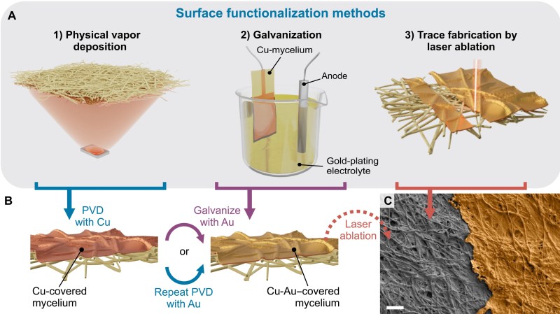
A notated illustration showing how a mycelial network may be functionalized as a PCB substrate. The process starts with Cu vapor deposition onto the network followed by Au either by more vapor deposition or electrodeposition. Traces are then cut via laser ablation.

E-waste is one of the main unfortunate consequences of the widespread adoption of electronic devices, and there are various efforts to stem the flow of this pernicious trash. One new …read more Continue reading MycelioTronics: Biodegradable Electronics Substrates from Fungi